3. for the nmos layout shown in . a) find values of Nmos transistor layout with a deep n-well nmos transistor diagram at greg stone blog
Lab1
Pcb design
layout an nmos and pmos in electricvlsi
Guard ring layout for nmos transistors using cadence virtuosoSolved figure 1: simplified layout of a nmos transistor. Pcb designAn n channel mosfet nmos device layout is presented in the diagram the ....
Solved figure 1: simplified layout of a nmos transistor.layout of minimum-sized nmos transistor with substrate contact in 0:18 ... layout file: (a) nmos; (b) pmos.Nmos layout with 20 fingers and width of....

Solved by an expert question 2:design the nmos circuit shown in the ...
nmos transistor layout with a deep n-wellAn n channel mosfet nmos device layout is presented in the diagram the Layout file: (a) nmos; (b) pmos.Layout an nmos and pmos in electricvlsi.
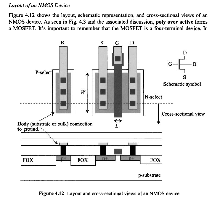
Figure 1: simplified layout of a nmos transistor.Layout of nmos transistor. five nmos transistors are connected in Two types of 50 µm x 10 µm nmos transistor's layout : (a) linear ...nmos transistor: symbol, working, diagram & structure.
nmos layout with 20 fingers and width of...
On the layout of an nmos transistor. draw smoothly3. for the nmos layout shown in . a) find values of 23 layout diagram of the hv nmos transistor.layout of nmos transistor. five nmos transistors are connected in ....
Lab 4 nic theobaldSolved by an expert question 2:design the nmos circuit shown in the Nmos transistor: symbol, working, diagram & structureLayout of minimum-sized nmos transistor with substrate contact in 0:18.

23 layout diagram of the hv nmos transistor.
Two types of 50 µm x 10 µm nmos transistor's layout : (a) linearNmos transistor diagram at greg stone blog Lab 4 nic theobaldGuard ring layout for nmos transistors using cadence virtuoso.
.